


Multiband Simulation of Quantum Transport in a Si Interband Tunneling Diode (ITD)
| GaAs DBRTD | Si ITD | type II RITD | Download |
 |
 |
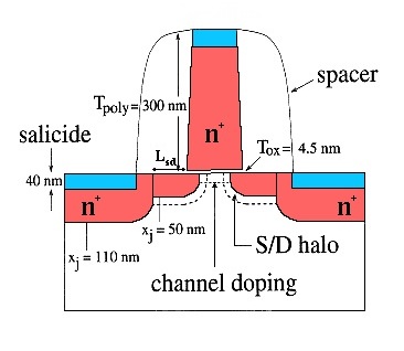
| Lg=25nm MOSFET, which may suffer with quantum effects. After D. Antoniadis et al.: www-mtl.mit.edu/Well/ |
Doping profile of the MIT MOSFET. |
 |
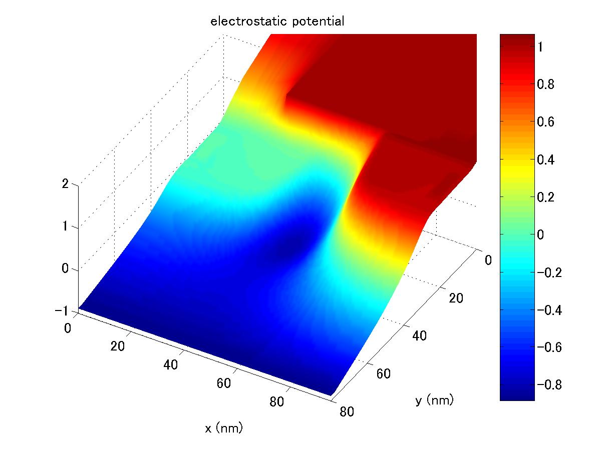 |
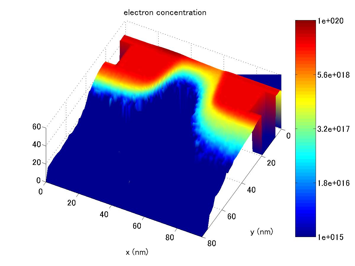
| Electron concentration in the MOSFET. | Potential Distribution. |
 |
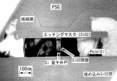 |
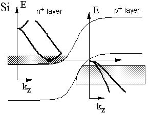
| Schematic band structure of Si ITD which makes use of the quantum effect. | Actual Si ITD developed by Panasonic (Mr.Sorada et al.) |
 |
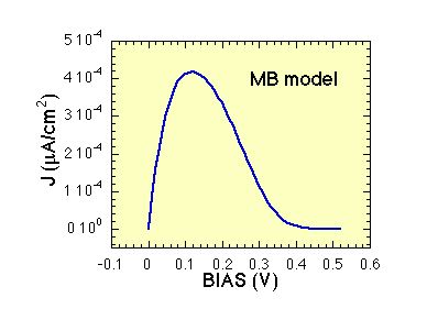 |
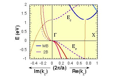
| Comparison of the complex band structuresof Si. Solid lines denote the multiband model(MB), while dashed lines two band model (2B). | I-V characteristics of the Si ITD simulatedby the MB model. for reference click here |
 |
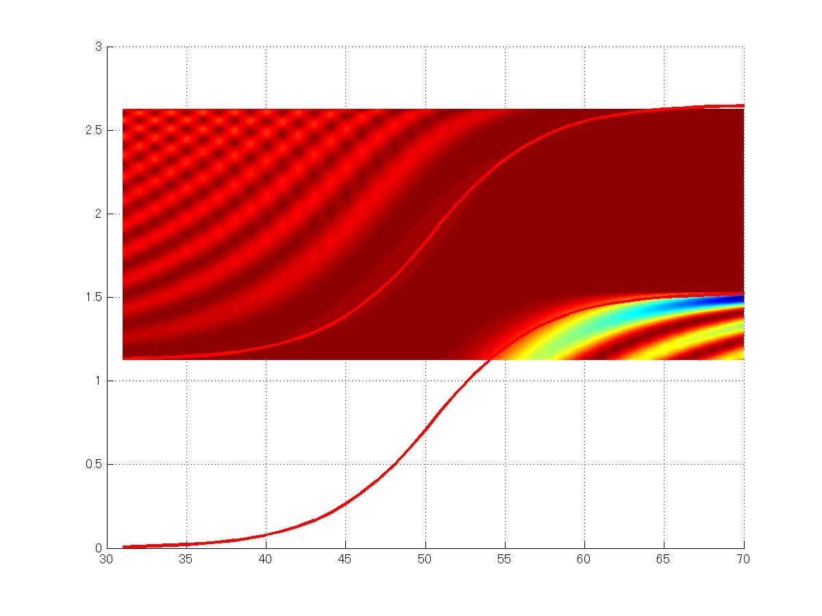 |
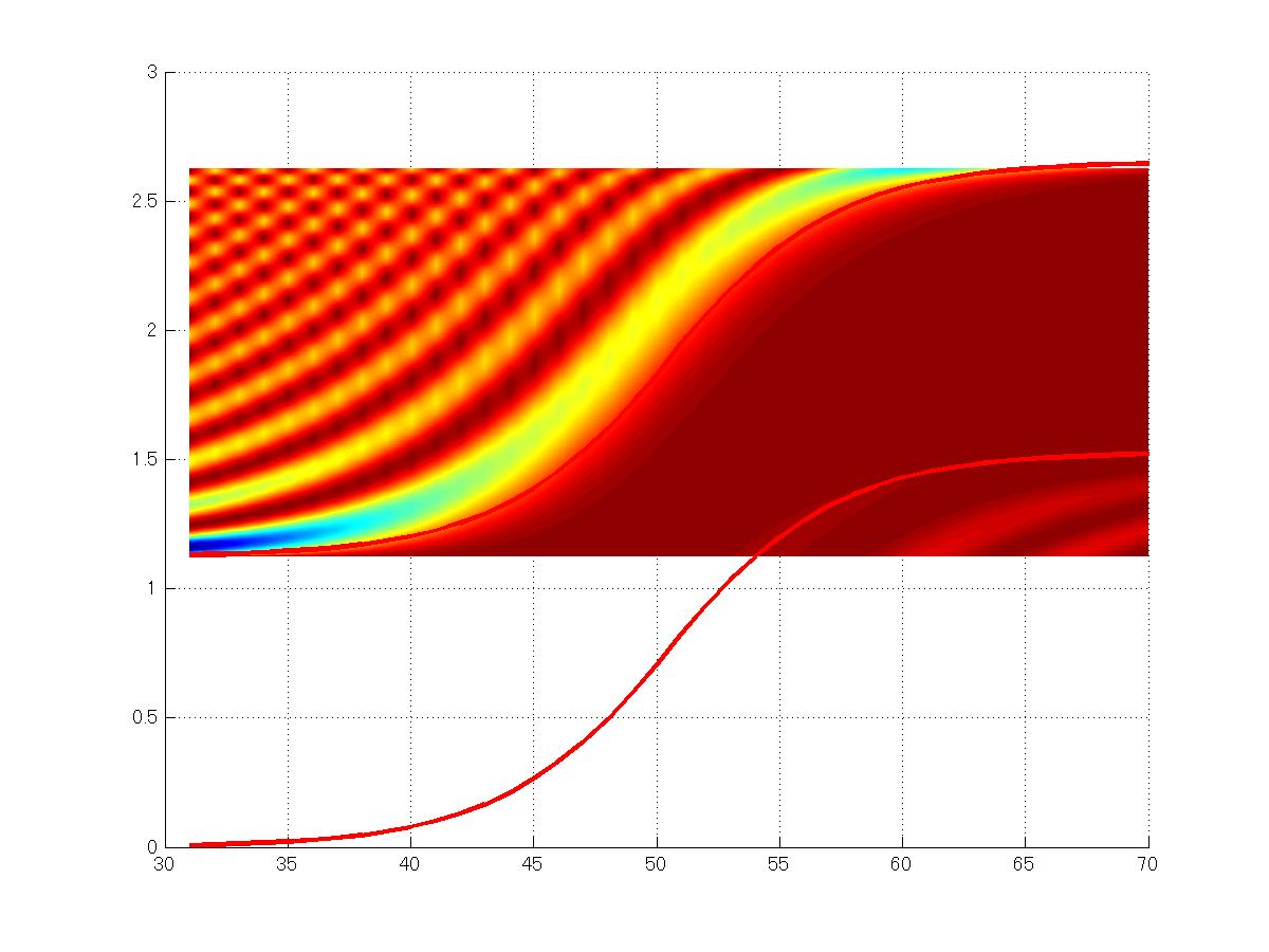
| Local density of states for the conductionband at the current peak. | Local density of states for both the CB andVB at the current peak. |
