


研究紹介
Computational Nano-Electronics (計算ナノエレクトロニクス)
計算ナノエレクトロニクスは,微細化された電子デバイスや光デバイスを構成する原子の個性をとらえつつ,電子や正孔の波の性質を考慮した新しい設計理論を構築し,実験を支えるとともに今後の研究開発をリードする研究分野です。(詳細は上のkeywordをクリックしてみて下さい. 対象は以下の通りです)
・ 次世代高効率量子ドット太陽電池の量子力学的設計
・ ナノスケールCMOSトランジスタの量子力学的シミュレータ開発
・ 新原理Siトランジスタの設計
・ 分子トランジスタ設計
・ 第一原理バンド構造計算に基づく新材料,新構造設計
・ 第一原理計算ソフトウェア(WIEN2k, VASP, CASTEP)の分かりやすいマニュアル
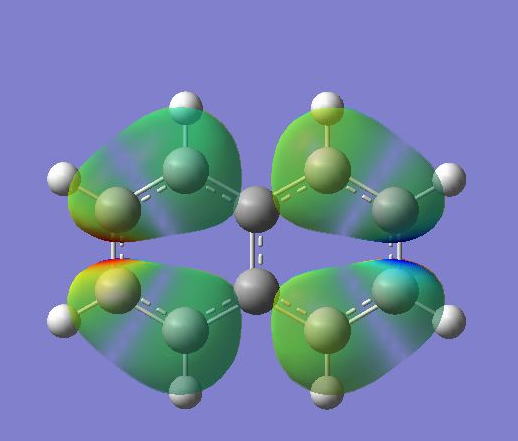
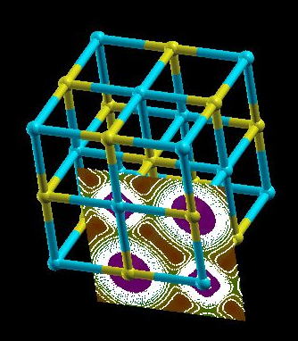
原子の個性をとらえて計算した例を絵で示してみました.
 |
 |
 |
| (a)Si 結晶の電子分布 | (b) 分子の分子軌道 | (c) NaCl の電子分布 |
 |
 |
| (d) Si の第一ブリルアンゾーンと 伝導帯の等エネルギー面 |
(e) 水素原子の各軌道の動径方向成分の極座標表示 |

Japanese
Vision Map (今後のデバイスの微細化の方向)
Parallel Computing (並列計算化技術)
(MPI, open MP,HPF, PVM, etc. in Quantum Transport Simulation, Molecular, and Ab Initio Band Calculation)
Multiband Simulation of Quantum Transport in Quantum Devices
(Based on the Multiband Green's Function Method)
GaAs/AlAs RTD: used for a terahertz microwave generation and high speed logic circuits with less device numbers compared with conventional logics used in SRAMs. Proper treatment of the material bandstructure properties, such as non-parabolicity, band-warping, and Gamma-X transistions.
Si ITD: suitable for device miniaturization below 25 nm gate length where most FETs suffer with quantum effects.
GaSb/InSb type II ITD: can be used for logics with high peak to valley current ratio.
Comparison of Tunneling Diodes(ITD, RITD, RTD)
2D and 3D Modeling (Quantum Wires and Quantum Dots)Corrugated Quantum Wire: high spatial density of QWRs on a (7 7 5) or (n n 1) oriented substrate with higher gain. (cooperative study with Prof. Hiyamizu's group who invented the structure).
Electronic States and Optical Properties of Quantum Dots: can be used for the optical lasers, sensors, memory and logic, as well as alternative computing concepts as quntum cellular automata.
A Lanczos code is used for a large scale matrix eigenvalue problem.
I am grateful for Dr. Jane A. Cullum at IBM T.J. Watson research center for her discussion.
I also thank Mr. Nestor Bojarczuk for his information.
Ab Initio Band Calculations (LSDA and GGA) and Tight-Binding Parameter Extraction(by a genetic algorithm)
InAs: material extensively studied for laser application.
GaN: material for blue light source and electronic devices at higher temperature.
Si: can be used for single / a few tens electron(s) memory and/or light source.
GaAs: material mostly used for high frequency FETs. We need the properties for the quantum transport simulation.
AlAs: we need the properties for the quantum transport simulation.
GaSb: we need the properties for the quantum transport simulation.
ITRS Modeling 2007 Update (日本語版:シミュレーションの部分のみ)
ITRS Modeling 2009 Update
ITRS